All the Small Things
Humans are always trying to breach the boundaries of the unimaginable. In recent years, thinking big has meant thinking significantly small, 10-9 meters small. Nanotechnology has fascinated many scientists from diverse backgrounds with its possible applications. From medicine to everyday electronics, our capabilities have enabled us to build atom by atom and thus, make enormous strides in science. Yet, this trend should come as no surprise. In 1959, Richard P. Feynman gave what could be seen as the catalyst of the nanotechnology age. In “Plenty of Room at the Bottom” he describes a bottom up way of thinking, building bottom up. Feynman expressed his surprise in the lack of nano scale work while simultaneously providing a waterfall of possible methods and applications.
Now, forwarding to the present day a significant amount of work has been done with nanotechnology. When we play with atoms themselves, we must account for weird outcomes. Probably the most popular example is the carbon nanotube. Imagine a monolayer sheet of carbon rolled into a cylinder. Depending on the parameters of the tube, the strength to density ratio can be quite impressive. This strength is due to the covalent sp 2 bonds between each carbon atom. Moreover, the electrical and thermal properties of these tubes also make it an exciting material. Recently, a research team at Rice University led by professors Junichiro Kono and Matteo Pasquali created wet-spun nanowires out of trillions of carbon nanotubes. These wires have proven superior to copper wires in electrical current carrying capacity, stiffness, and convenience, as it is extremely light and thinner than a strand of human hair. Overall, these fibers can carry four times more current than copper wiring of the same mass.

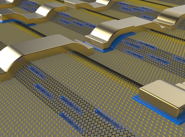
Scientists have also turned towards nanoribbons composed of graphene, a 2D crystal lattice one atom thick. This material can be considered the “star” of the nanotechnology world, with many scientists working on maximizing the material’s capabilities. Recently, a study led by Georgia Institute of Technology professor, Walt de Heer, presented epitaxial graphene nanonribbons grown on silicon carbide that actually conducts electricity at room temperature ten times better than theoretical predicted. Moreover, compared to exfoliated grapehene, we see an increase in conduction length by 1000 times at an impressive >10 micrometer distance. Interestingly, the nature of the flow of electrons along the sides of these ribbons resembles that of photons through an optical fiber. Sleek when you think of the scattered electron paths inside a standard conductor.
At Notre Dame we have our own Nanofabrication Facility, complete with those flattering clean room gowns. I am currently working on growing my own recipe for a novel semiconductor material using MoS2 and WS2. Though it may seem like graphene has a monopoly on the hearts of scientists and engineers working on nanoelectronics, its lack of a band gap, and subsequent leaking current, restricts its use as semiconductor material. Thus, transition metal oxides and sulfides have come onto the seen due to the band gaps they possess. This results in a decrease in the amount of energy lost as well as the size of the electronics the material will be used in. The most successful method for growth has been chemical vapor deposition, which includes precursors and a substrate. Generally, the precursors are vaporized to combine and depose on the substrate to form the desired substance. One can control the shape and the thickness of the crystals by altering the temperature, pressure, amount of precursor, and time.
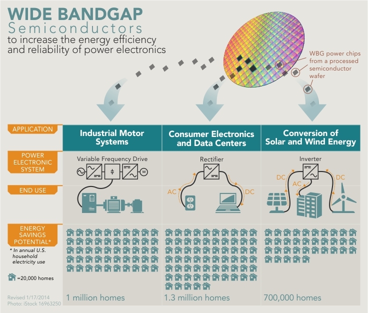
Even the government has begun to praise the value of wide band gap semiconductors. Earlier this year, President Obama announced the Department of Energy’s new manufacturing innovation institute focused on the proliferation of WBG semiconductors. The main motivation of the institute lies in the environmental benefits that result from the reduction, approximately 75-80%, in electronic heat waste. This is a significant stride in the enthusiasm for nanelectronics as it now resides within the intersection of science and government.
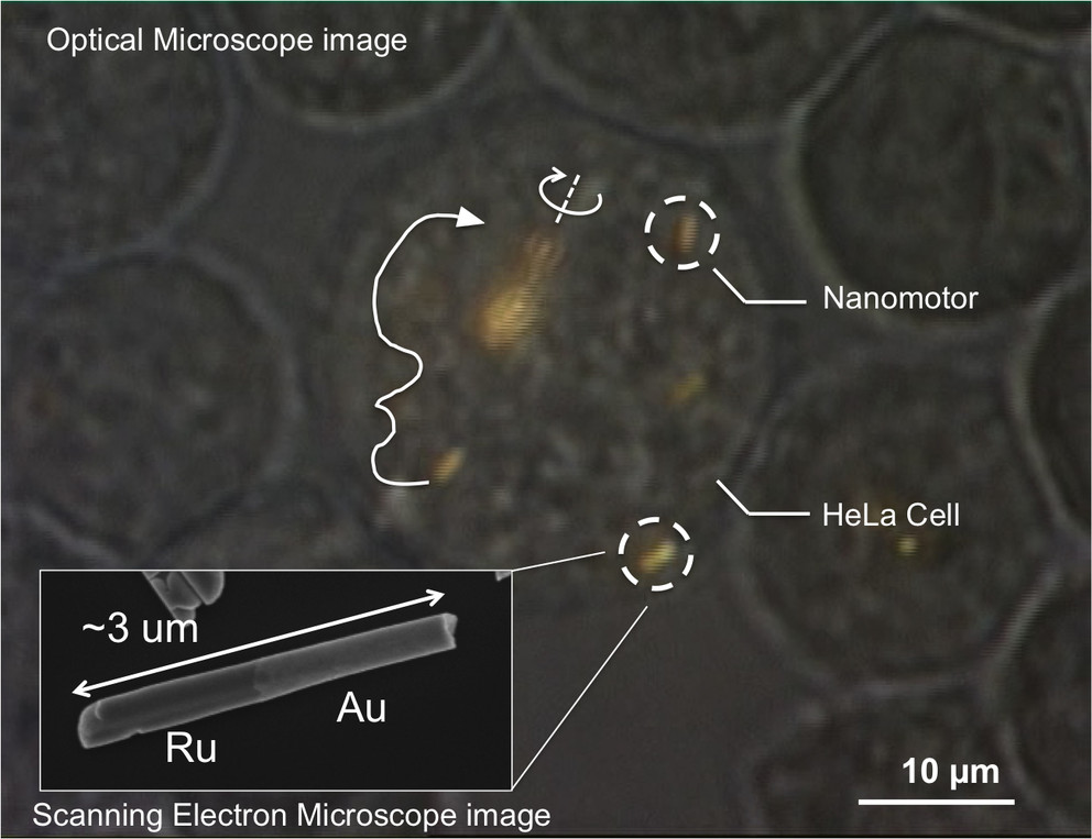
Nanotechnology obviously has an outstanding future in electronics, but I should also mention some of its medical promises. Scientists have worked with nanoshell solutions and lasers to replace traditional suturing as well as with nanowires that can electronically identify the proteins present during the early signs of cancer. Though I could list many medical studies in this one post, and I encourage the interested reader to look through the many online papers, I believe it is better to highlight a recent development that is both amazing and creepy. A group at the Pennsylvania State University has, for the first time, succeeded in placing gold-ruthenium nanomotors into living HeLa cells. Through the use of ultrasonic waves, the team was able to magnetically control the motors and watch as they interact with the cellular membranes. As uncomfortable as it is to think of several of these tiny bots constantly playing bumper cars with your cells, the ramifications of this breakthrough are actually quite inspiring. Using this nanotechnology we have better chances of targeting and destroying cancers cells, improving patient diagnosis, delivering noninvasive drugs, and even performing cellular surgery.
Scientists and engineers are often asked to predict the future of technology. Where will we be in 50 years? Will science fiction become a norm? Even companies have taken it upon themselves to give the public a taste of their compelling, though somewhat ambitious future predictions. Samsung has been boasting their flexible screens for a little over a year now and yet; none of these products have come onto the market. Ultimately, we have not refined these products well enough. Time is still needed to make these tech dreams come true.
As a junior physics major, still dreaming of a lab of my very own, I am excited with where science and engineering is headed. We now have the capabilities to manipulate atoms; we can now be more creative than ever. The brilliant minds before us were able to combine materials into products that advanced our lifestyles as well as our knowledge of the surrounding Universe. With nanotechnology the current generation of scientists and engineers can use the inventions of the past to create new and better materials. Combine child like curiosity and imagination with mature scientific knowledge and mankind experiences ingenious discoveries.
References:
- Baringhaus, J., & Ruan, M. (2014). Exceptional ballistic transport in epitaxial graphene nanoribbons. Nature, Retrieved from http://www.nature.com/nature/journal/v506/n7488/full/nature12952.html
- Feynman, R. P. (1959). Plenty of room at the bottom. Retrieved from http://www.pa.msu.edu/~yang/RFeynman_plentySpace.pdf
- Gibney, E. (2014, February 06). Graphene conducts electricity ten times better than expected. Retrieved from http://www.nature.com/news/graphene-conducts-electricity-ten-times-better-than-expected-1.14676
- Kahn, J. (2006, June). Nano’s big future. National Geographic, Retrieved from http://ngm.nationalgeographic.com/2006/06/nanotechnology/kahn-text/1
- U.S. Energy Department. (2014, January 16). Next-generation power electronics: Reducing energy waste and powering the future. Retrieved from http://energy.gov/articles/factsheet-next-generation-power-electronics-manufacturing-innovation-institute
- Weidner, K. (2014, February 10). Nanomotors are controlled, for the first time, inside living cells. Retrieved from http://news.psu.edu/story/303296/2014/02/10/research/nanomotors-are-controlled-first-time-inside-living-cells
- Williams, M. (2014, February 13). Rice’s carbon nanotube fibers outperform copper. Retrieved from http://news.rice.edu/2014/02/13/rices-carbon-nanotube-fibers-outperform-copper-2/